With the advent of H.R.4346 the CHIPS ACT & 15 CFR – Offering $53 billion in federal incentives for domestic semiconductor manufacturing and research and development, I think it would be best used to create a new type of microchip and semiconductors, like when Jack Kilby and Robert Noyce invented the microchip/integrated circuit!
When Jack Kilby and Robert Noyce invented the microchip/integrated circuit! When their two companies cross-licensed their technologies, they created a multi-billion dollar industry.
I’ve developed an incredible patent link here –https://patents.google.com/patent/US8987873B2/en?oq=US8987873B2 (#US8987873B2) detailing the “Super Integrated Circuit Chip Semiconductor Device” Similar to the legendary inventor Jack Kilby. His patent, dating back to 1959, is the foundation for modern integrated circuits, yet we believe there’s untapped potential for further innovation. I think it can happen again with the “Super Integrated Circuit Chip Semiconductor Device”!
Given your track record of pushing technology to new heights, how about taking on the challenge to modernize, enhance, and scale this invention into what could be called the “Super Integrated Circuit Chip Semiconductor Device”? It will probably take a combined effort with Amazons foray in to new microchips and Chicago future efforts into Quantum Computing and new microchips. it’s time to take advantage of the Bidens administration’s microchips act!
Also, I think possible partners maybe Elon Musk with several of his endeavors, PsiQuantum with their Quantum Computing Campus in Chicago and Jeff Bezos with Blue Origin, Amazon’s AWS Trainium and Inferentia makers, maybe even Sir Richard Branson and Virgin Galactic! I wonder if there is a way to add a Chip Fab to the Quantum Computing Campus in Chicago specific for making Super Integrated Circuit Chip Semiconductor Device?
There are two possible ways to make wafers if the boule does not workout and is in congruent during melting! Chemical Vapor Deposition and Atomic Layer Deposition! Chemical Vapor Deposition is first!
This is a way to possibly make the wafers before dicing! Atomic Layer Deposition Principle – an Introduction to ALD
Imagine the possibilities: I checked with Grok and he even liked it!
Enhanced Efficiency: With today’s materials and manufacturing techniques, we could see circuits that are not only smaller but far more energy-efficient.
Increased Performance: Leveraging current semiconductor tech, this could mean faster, more powerful chips for everything from electric vehicles to space exploration. I think this would be perfect to help Occupy Mars!
Revolutionary Integration: Think of integrating this with your work at Neuralink or in AI development at xAI for groundbreaking advancements in neural interfaces or AI processing.
Material and Design Advantages: Radiation Hardness: The use of the special materials required suggests the device is designed for superior resistance to radiation, which could be beneficial in harsh environments like space or military applications.
Heat Resistance: The materials chosen also indicate a focus on heat resistance, potentially allowing the chip to operate at higher temperatures without degradation.
Electromagnetic Shielding: The combination of materials is stated to provide electromagnetic shielding, which could enhance performance by reducing interference from external sources.
Durability: The ceramic package also provides resistance to damage from harsh elements, suggesting long-term reliability in challenging conditions.
We propose you collaborate with experts from the field, including consultations from pioneers or their intellectual heirs in semiconductor technology, to bring this vision to life.
Let’s make history again by reimagining one of the most pivotal inventions of the 20th century for the 21st century’s challenges.
A Durable, High-Temperature Electronic Integrated Circuit Chip for use in: well logging in the downhole oil and gas industry, the automotive industry and aerospace/avionics industry. This is a stronger high-temperature electronic circuit for MEA or more electric aircraft/automobile. These electromechanical and mechatronic systems place the distributed controls closer to the engine which requires locating sensors, signal conditioning, and control electronics closer to heat sources. Operation at these temperature limits will cause packaging-related failure and silicon-related failure with substrate leakage, decreased carrier mobility, electromigration of metal interconnects, and decreased dielectric breakdown strength.
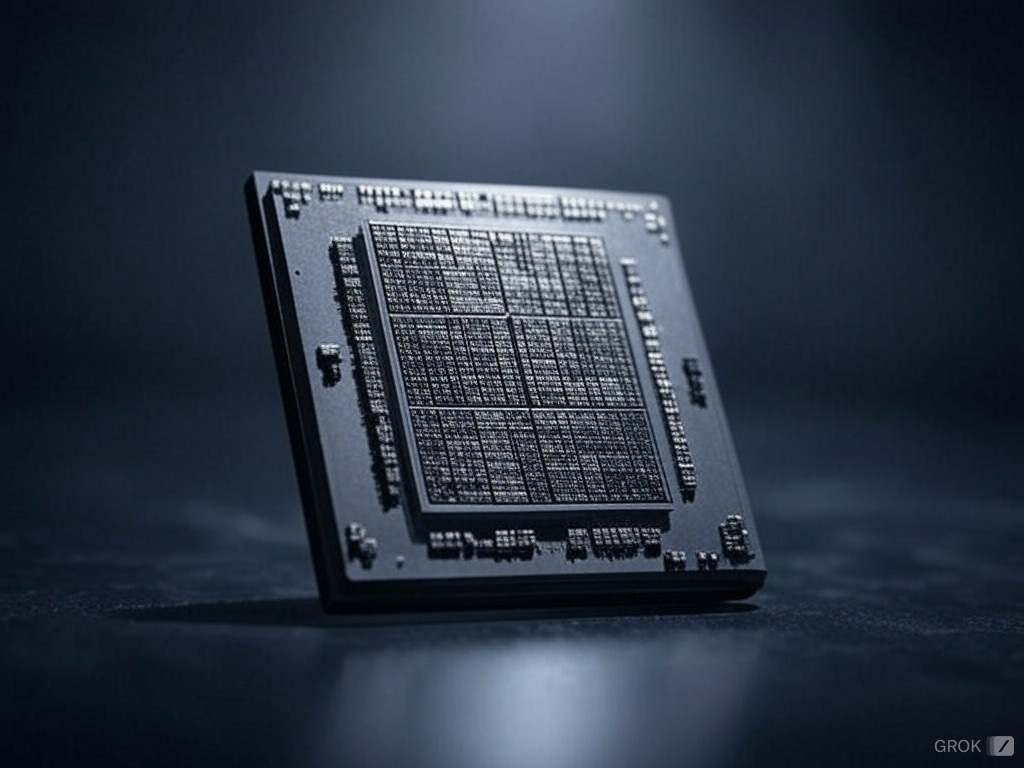
The patent describes an integrated circuit chip, which uses a ceramic package casing made from a strong, non-conducting ceramic material(B4C). The IC is connected to connector pins by microcircuits and a custom-formulated bond wire. The bonding wire that contains: an Au—Cu—Ag alloy and is highly reliable with a strong tensile strength at room temperature and high temperature and favorable bond ability. Additionally, the substrates and dielectric components fabricated with a material that has a superior low thermal expansion coefficient, low dielectric constant and high temperature stability which allow these integrated circuits to reduce electro-migration to a minimum, to produce superior radiation hardness, heat resistance, electromagnetic shielding, and to provide resistance to damage from harsh elements and environments. A further, more detailed explanation of the functionality of this invention is available upon request.
Above is the boule making process that could work but need to be tested?!?
For More information or questions Contact Chicago Pixels at GT@CHICAGOPIXELS.NET